Single sided PCB milling

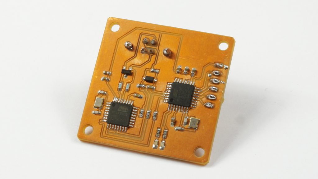
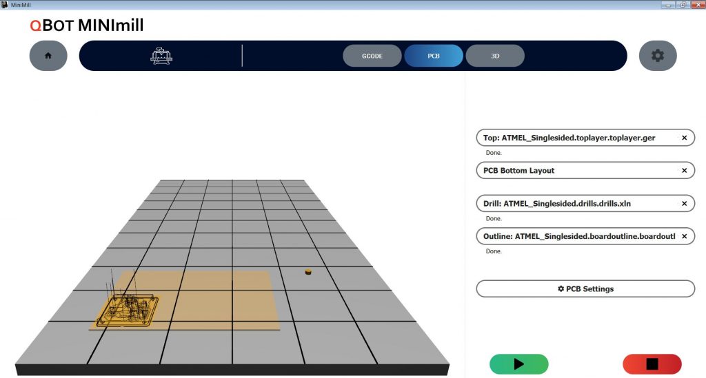
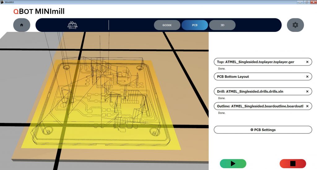
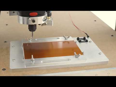
Your MINImill can manufacture single or double sided PCBs from GERBER files. The following tutorial covers single sided pcbs.

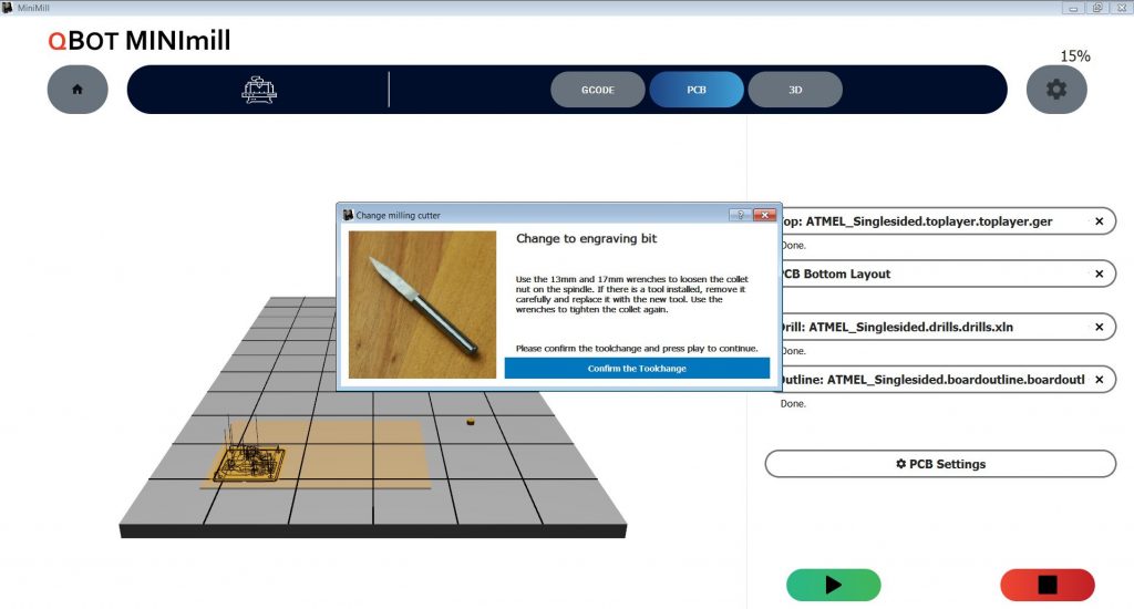
In order for the tool change and the automatic height adjustment to work with your MINImill, we recommend the PCB clamping holder. Alternatively, you can also connect the circuit board directly to the controller. The necessary wiring is described in the instructions for the clamping holder or the tool length sensor.

Open GERBER files

Your MINImill software can open Gerber files directly in the PCB tab. We have tutorials with the appropriate settings for Eagle, Kicad and Altium. You can find the instructions for the PCB programs in our wiki.

You can mill the following GERBER files:

  • PCB Top Layout respectively Top: Top Layer
  • PCB Bottom Layout respectively Bot: Bottom Layer
  • PCB Drill File respectively Drill: Drill.xln
  • PCB Outline respectively Outline: Board outline Gerber
  • Please note: The PCB outline must have a width greater than 0 and be closed. Line widths with the value 0 are ignored. We recommend removing texts or logos before milling.

    Please note, that single-sided circuit boards can only be milled without a bottom layer. As soon as the Bottom Layer file is loaded, it automatically switches to double-sided circuit board milling. You can mirror your Bottom file to be milled as the top layer in the GERBER export of your PCB program.

    You can move and position your board on the PCB surface. Under the PCB settings you can change the dimensions and the positioning of the PCB holder. We have separate assembly instructions for the PCB holder under the following link:

    PCB holder instructions

    Start the milling process

    After clicking on the green start button, the milling machine starts the circuit board milling process in the following order:

  • Clamp the PCB engraving bit
  • Tool length measurement
  • Surface scan for automated height adjustment
  • Engraving
  • Tool change to the first drill bit
  • Drill File drilling
  • Tool change to the PCB outline cutter (2mm PCB end mill)
  • If the surface scanning (probing) does not work, please check the electrical wiring (5V probe pin should be pulled to GND when there is a contact – connection description in the PCB clamping holder tutorial is identical to the tool length sensor wiring).

    PCB milling process

    Follow the software instructions during the milling process. We recommend vacuuming the chips with a vacuum cleaner after finishing the PCB milling process.

    We recommend cleaning the circuit board with circuit board cleaner before further use. This removes the protective layer on the circuit board and allows you to solder the circuit board easily.

    You can either seal the circuit board with a solder able protective coating before soldering or clean it after the soldering process and seal it with a protective coating (clear coating, ESD coating,…).